Expert contributors for this post
Dr. Andrew Tweedie
UK Director & Co-founder
Rahul Nagaraja
Multiphysics FEM Software Developer
Introduction
Fingerprint sensors play a crucial role in modern security and identification systems. From smartphones and laptops to industrial and governmental applications, biometric fingerprint sensing has become one of the most commonly used authentication methods due to its reliability, ease of use, and compact integration capabilities. Among the technologies used in fingerprint sensing, Piezoelectric Micromachined Ultrasonic Transducers (PMUTs) stand out due to their small footprint, energy efficiency, and scalability in sensor arrays.
However, PMUTs, like other MEMS devices, are highly sensitive to process variations introduced during fabrication. These variations can include changes in material thicknesses, lateral dimensions, and other geometric features. While deterministic simulations help in understanding the ideal performance of the device, they often fall short in predicting how real-world imperfections affect functionality.
This is where Monte Carlo analysis becomes essential. By evaluating thousands of slightly varied designs based on expected manufacturing deviations, engineers can statistically estimate production yield, detect sensitive dimensions, and gain deeper insights into robustness and reliability. Unfortunately, such analysis traditionally requires significant computing resources and time, limiting its practicality.
This blog explores how Monte Carlo simulations of a PMUT fingerprint sensor become feasible and efficient when powered by Quanscient Allsolve’s cloud-based simulation capabilities. With its parallel parametric sweep feature Allsolve makes large-scale statistical analysis not only possible but practical within a tight design cycle.
Impact of Quanscient Allsolve on Monte Carlo analysis
Monte Carlo analysis typically involves hundreds or thousands of individual simulations, each representing a different combination of possible manufacturing variations. In conventional workflows, running these simulations sequentially can take several days or even weeks, depending on the complexity of the physical model involved.
Quanscient Allsolve changes the equation entirely. As a cloud-native multiphysics simulation platform, Allsolve leverages scalable compute resources to run massive simulation batches in parallel. Its parallel parametric sweep capability allows users to submit hundreds or thousands of design variations, all processed simultaneously, dramatically reducing the total runtime.
In this study, 1,000 randomized geometries of a PMUT sensor were simulated in under 15 minutes. The same workload would require over two days of continuous computation if processed sequentially. This efficiency opens up new design possibilities and enables statistical validation within normal development timelines.
Finally, Allsolve supports strongly coupled multiphysics interactions, essential for accurate modeling of PMUT devices. Piezoelectric behavior, acoustic wave propagation, and elastic deformations are all evaluated simultaneously in a single simulation framework, yielding highly realistic results.
Quanscient Allsolve
Array-scale cloud based MUT simulations
Natively coupled PMUT and CMUT simulations with Quanscient Allsolve
Case study
Monte Carlo analysis of a PMUT based fingerprint sensor
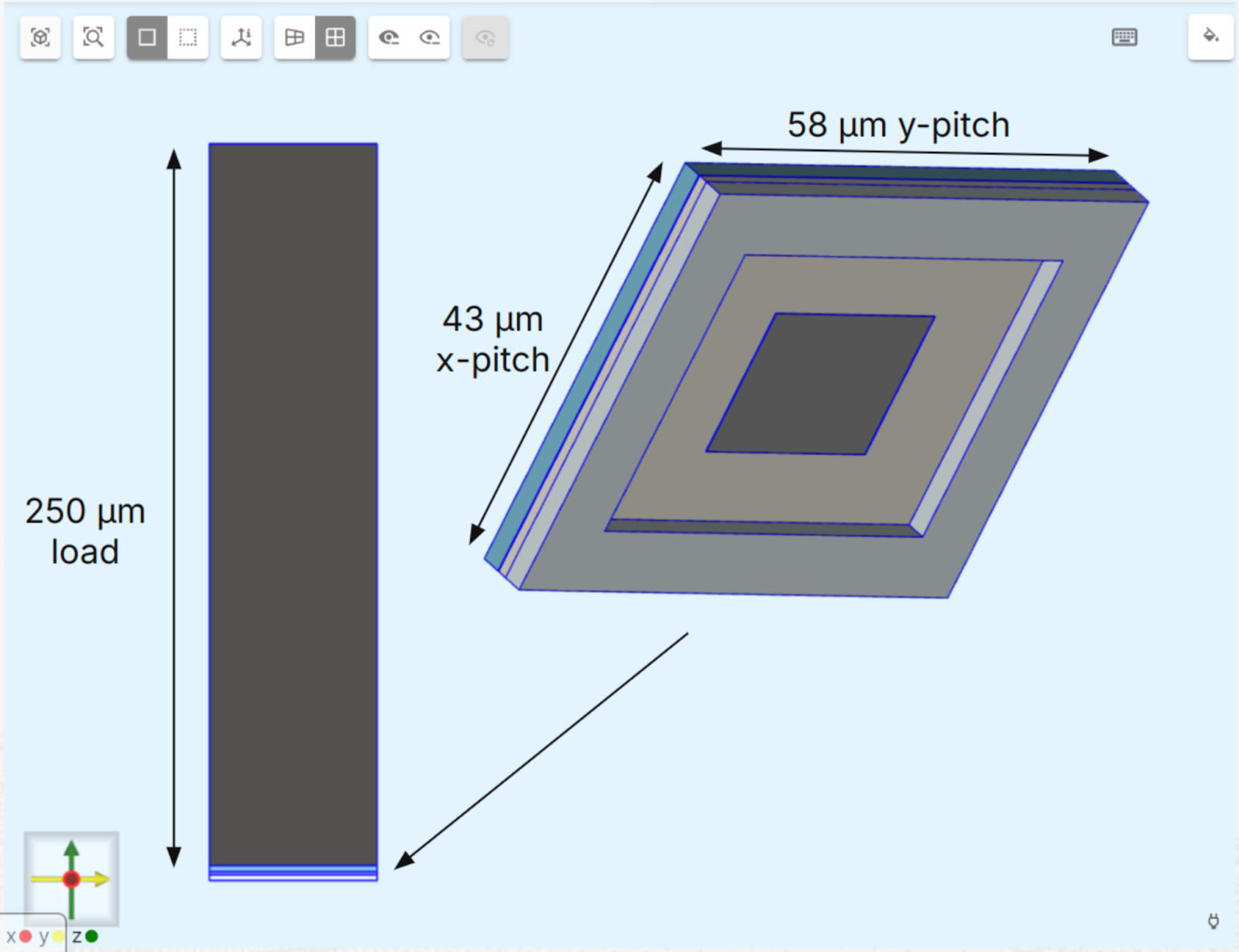
The case study centers on a single PMUT element used in a fingerprint sensor array. The device architecture features a layered stack of materials, each playing a critical role in its function. From bottom to top, the layers include:
-
A silicon dioxide (SiO2) layer with an etched cavity
-
A bottom electrode made of molybdenum
-
A piezoelectric layer composed of aluminum nitride (AlN)
-
A top electrode made of aluminum
-
A silicon elastic layer
-
A polydimethylsiloxane (PDMS) acoustic load layer
Fig. 1 PMUT element stack considered for Monte Carlo analysis
The operating principle of the PMUT is straightforward but involves complex physical interactions. A voltage is applied across the piezoelectric layer, inducing mechanical vibrations. These vibrations propagate through the device and are transmitted into the PDMS layer as acoustic waves. Reflected signals from the top surface are then captured, and their characteristics (amplitude and arrival time) serve as indicators of performance.
The objective was to assess how variations in geometry, as introduced during manufacturing, affect these performance indicators. To do this, seven key dimensions were selected for random variation. These included lateral cavity dimensions and the thicknesses of the oxide, electrodes, and elastic layers.
Random variations followed a normal distribution, representing common manufacturing tolerances. For each of the 1,000 design variations, a complete transient simulation was run, capturing the response over 300 time steps and solving approximately 380,000 unknowns per run.
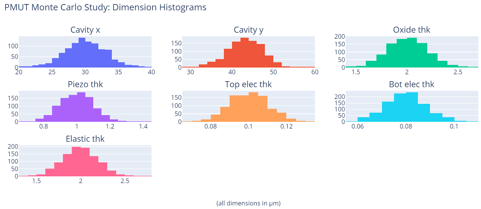
Fig. 2: 1,000 random variations of the single element PMUT stack. Each key dimension is randomly altered, following a normal distribution. The distribution around the mean value can be adjusted by setting its coefficient of variation (CV)
Simulation objective
The primary goal of the simulation was to predict the statistical impact of geometric fabrication variations on key performance indicators (KPIs) for a PMUT fingerprint sensor. In particular, the study focused on two measurable aspects of the received voltage signal:
- Signal amplitude: a key determinant of image sensitivity
- Arrival time: crucial to control for accurate beam forming to achieve high spatial resolution
Monte Carlo analysis was selected as the most appropriate method for this investigation due to its ability to capture stochastic behaviors arising from geometric uncertainty. The idea was to replicate a realistic manufacturing scenario by generating 1,000 design instances with slight geometric deviations, then measuring how those deviations affected performance.
These performance indicators were evaluated against predefined pass/fail criteria. A simulation was marked as a failure if:
- The amplitude deviated by more than ±50% from a nominal value of 0.8 nA
- The arrival time deviated by more than ±1% from a nominal value of 660 ns
This approach allowed for a data-driven estimation of yield, the percentage of devices expected to meet performance standards despite fabrication variations.
The model
Each simulation incorporated detailed, strongly coupled multiphysics modeling. The physical domains and couplings involved were as follows:
- Electrostatics in the piezoelectric layer, driven by applied voltage across electrodes
- Elastic wave propagation in all structural layers (except PDMS)
- Acoustic wave propagation in the PDMS load layer
The simulation domain included boundary conditions tailored to capture realistic behavior. The bottom of the oxide layer was fixed to simulate anchoring, while two lateral surfaces used symmetry conditions to reduce computational complexity. A perfectly matched layer (PML) on the top surface of the PDMS absorbed outgoing acoustic waves to prevent artificial reflections. The remaining PDMS lateral surfaces were pressure-neutral.
Two major multiphysics couplings were modeled:
- Acoustic-structure interaction (ASI): coupling between elastic waves in the solid layers and acoustic waves in the PDMS
- Piezoelectric coupling: interaction between electrostatic and elastic fields within the AlN layer
Each simulation involved time-stepping the system to capture the full response of the sensor. With 300 timesteps and approximately 380,000 unknowns per model, this analysis required significant computational power, another reason parametric sweeps via Allsolve was essential.
Key results
Simulation outputs showed a wide range of responses due to geometric variations. The most immediate observation was the diversity in current vs. time plots. Echo signals from different simulations showed varying amplitudes and arrival times, clearly indicating the effect of dimensional changes.
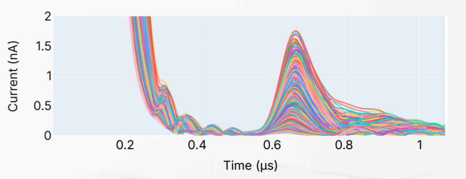
Fig. 3: Current Envelope over time received from each of 1,000 simulations, showing a clear reflection from the front face of the PDMS.
Cross plots comparing geometric dimensions to KPIs revealed strong correlations for certain parameters. For instance, variations in oxide layer thickness showed a notable impact on arrival time, while cavity dimensions had a greater influence on amplitude. Such insights are invaluable for design optimization and identifying critical manufacturing controls.
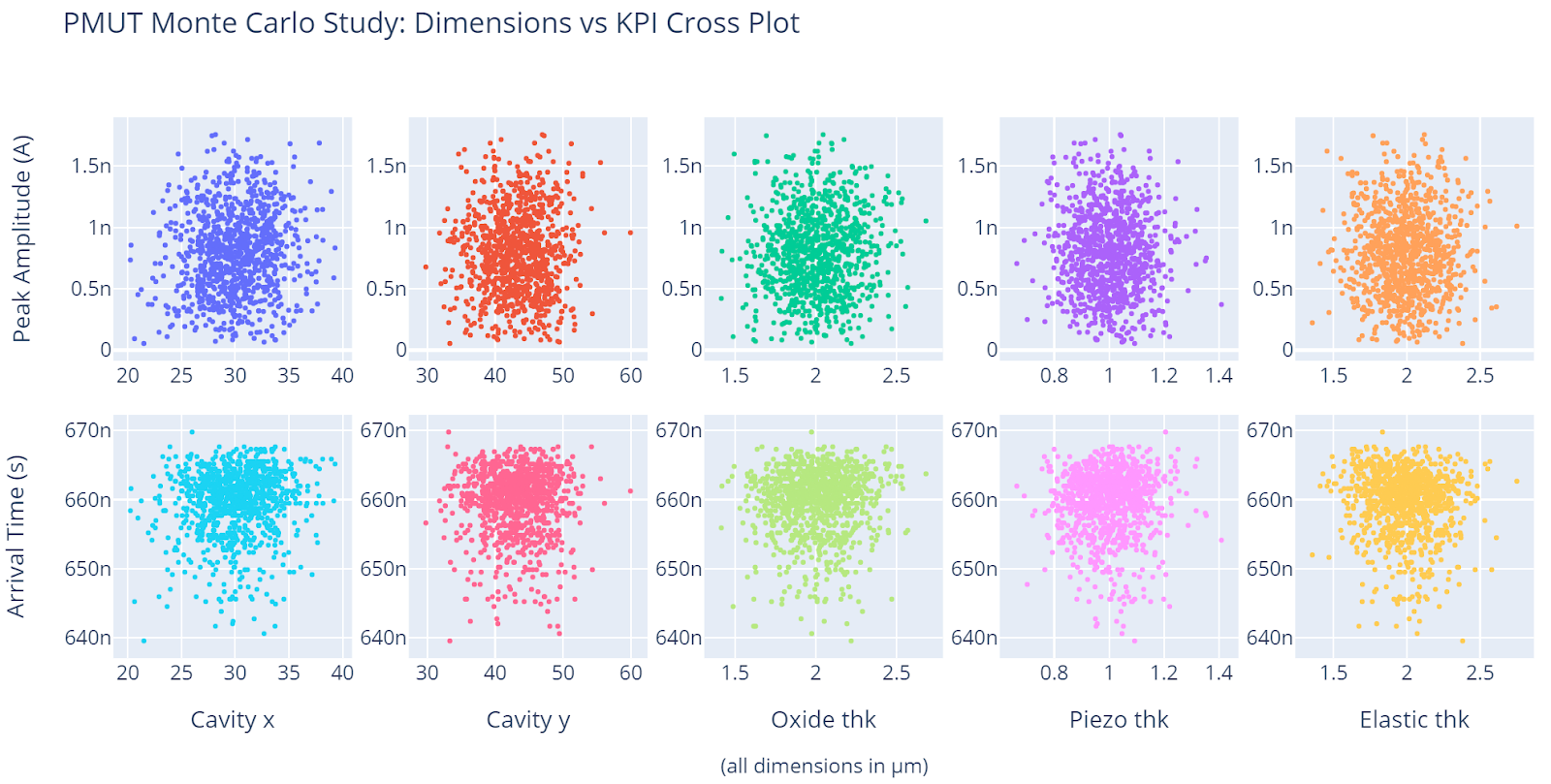
Fig. 4: Cross plot of dimensions (x-axis) vs KPIs (y-axis) for 1,000 simulations
The KPI histogram analysis provided a quantitative look at performance distribution. Applying the defined pass/fail criteria:
- 252 out of 1,000 simulations failed the amplitude test
- 135 simulations failed the arrival time test
With some simulations failing in both amplitude and arrival time, the total simulations that failed the KPIs were found to be 281, leading to an estimated yield of 71.9%. This is a realistic and useful number that can guide both design improvement and manufacturing decisions.
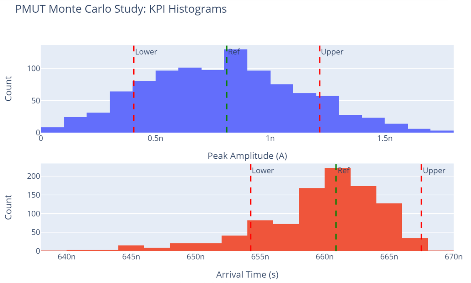
Fig. 5: KPI Histograms from the Monte Carlo study. Notice that despite the use of normal distributions on the input dimensions the arrival time distribution has a very different shape.
The runtime data is equally compelling. With each simulation taking about 4 minutes, a sequential approach would require over 66 hours. In contrast, Allsolve’s parallel parametric sweep completed the full batch in just 15 minutes - a 260x speedup.
Key benefits demonstrated
This case highlights several significant benefits enabled by Quanscient Allsolve:
- Speed: The simulation time reduction from over 2 days to 15 minutes allows engineers to incorporate Monte Carlo analysis in routine design workflows.
- Depth of insight: By running 1,000 simulations, engineers gain statistically robust insights into device behavior, far beyond what deterministic simulations can offer.
- Design confidence: Identifying which parameters most influence KPIs allows for better tolerance allocation and design rules.
- Early yield prediction: Engineers can estimate yield before any physical fabrication, potentially saving time and cost.
- Complex physics handled together: Strongly coupled multiphysics simulations ensure accurate representation of real-world behavior, including electrostatic, elastic, and acoustic effects.
Conclusion
Monte Carlo analysis provides an essential window into the effects of manufacturing variability on MEMS device performance. For applications like PMUT-based fingerprint sensors, where precision and reliability are critical, understanding how small geometric differences impact signal quality and timing is key to successful design.
In this blog, we demonstrated how Quanscient Allsolve makes this kind of statistical analysis practical. By reducing simulation time from days to minutes, and by supporting complex, coupled physics models, Allsolve enables engineers to build more reliable devices, faster.
The ability to evaluate design robustness and predict yield before fabrication is not just a time-saver, it's a game-changer for MEMS and sensor innovation.
Engineers and product developers no longer need to choose between speed and accuracy. With Allsolve, they can have both.
References
[1] Jiang, Xiaoyue, et al. "Ultrasonic fingerprint sensor with transmit beamforming based on a PMUT array bonded to CMOS circuitry." IEEE transactions on ultrasonics, ferroelectrics, and frequency control 64.9 (2017): 1401-1408.
[2] Halbach, Alexandre. "Domain decomposition techniques for the nonlinear, steady state, finite element simulation of MEMS ultrasonic transducer arrays." (2017).